astrorat.com

Adding a RS232 Interface to the H8-5 Cassette Interface

My first attempt using the H8-5 Cassette Tape and Serial Board to load H8T files
The first serail interface
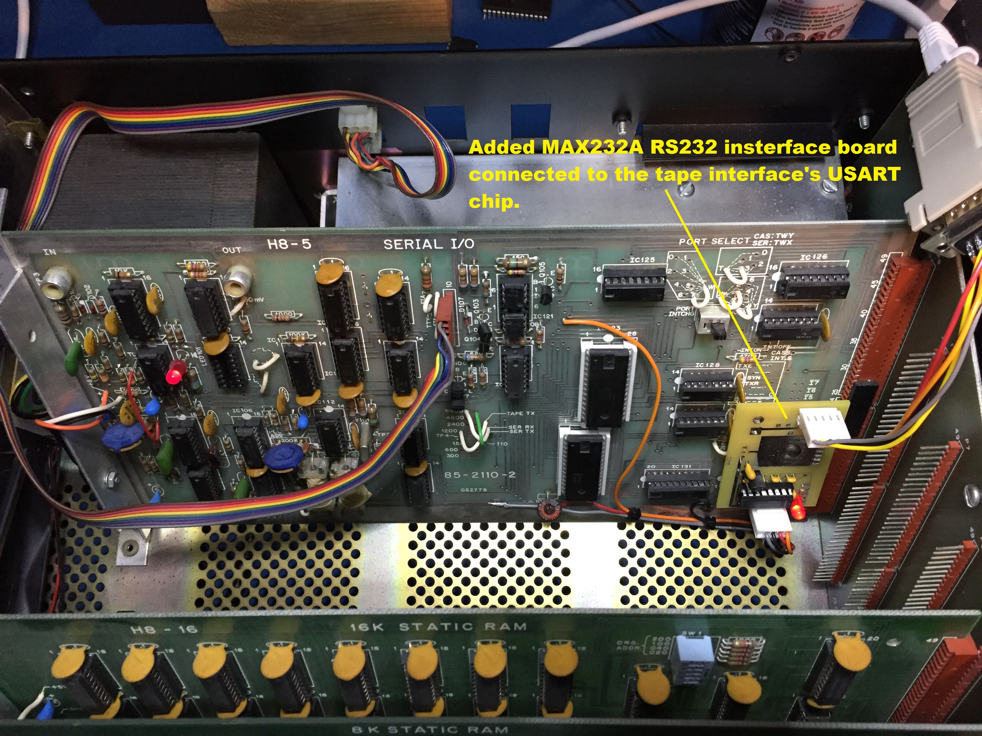
The H8 system I received came with the H8-5 cassette/serial interface card. While I tested the cassette interface using one of the lab cassette recorders to write and then read back a tape, it became clear to me that finding working 35+ year old tapes for the H8 would be some what of a challenge. Even if I locate anything, the age of these tapes would most likely reveal that any data stored on them to be quite dicey to read back. Another solution would need to be developed.

For my first attempt, the solution came in some form of a card being added to the H8-5 card. This extra card 
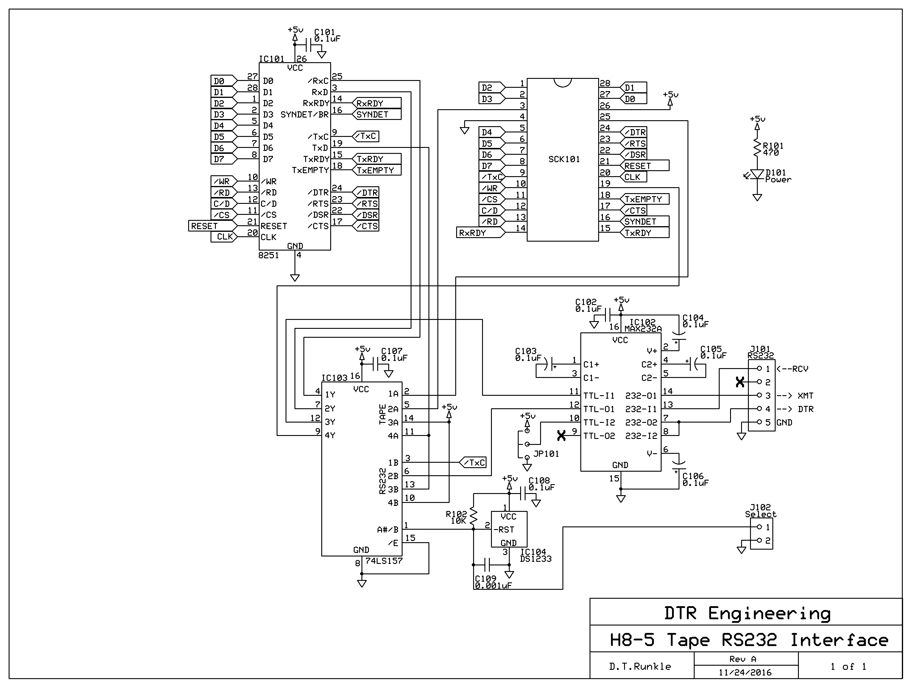
creates a standard RS232 interface between the H8-5's tape interface circuit and a PC.

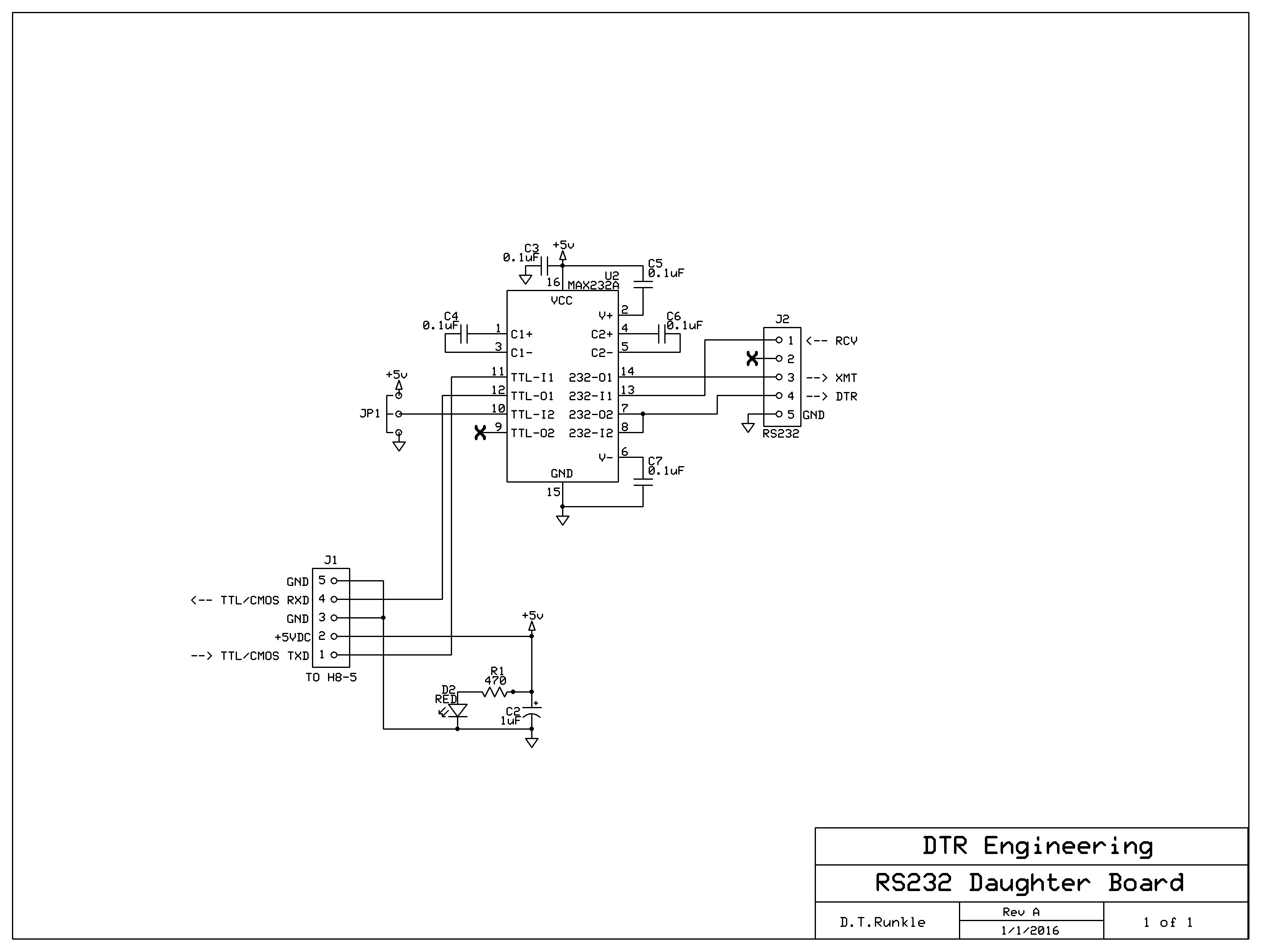
As it tuned out, I already had such a card designed for one of my other projects. This card had two 5-pin connectors for power plus TTL/CMOS signals and another for the RS232 interface.

The picture above shows the modification. Also note the standard DB9 connector that returns to my lab's PC where I read/write H8T program files.

As mentioned earlier this board came form another of my projects. Over time I have been designing and restoring computers based around the RCA 1802 microprocessor used in the COSMAC Elf articles in 1976 and 1977. One of the more resent Elf's designs I has acquired was the Membership Card by Lee Hart.

I ended up designing an interface card to both power and provided RS232 interfacing for my Membership card. Using this card as a starting point I updated it to be used as the first generation interface board to connect the H8-5's tape electronics to an RS232 serial connection ending at one of my PCs.

In the original Member Card version, I had a DC power connector that ran to an on board analog +5 volt DC regulator circuit. Since I was going to pull +5 volt DC straight from the H8-5 card, I had no need for the parts used in this portion of the circuit.  I just left the parts off the board leaving empty holes.

The following schematic show the resulting daughter board design.
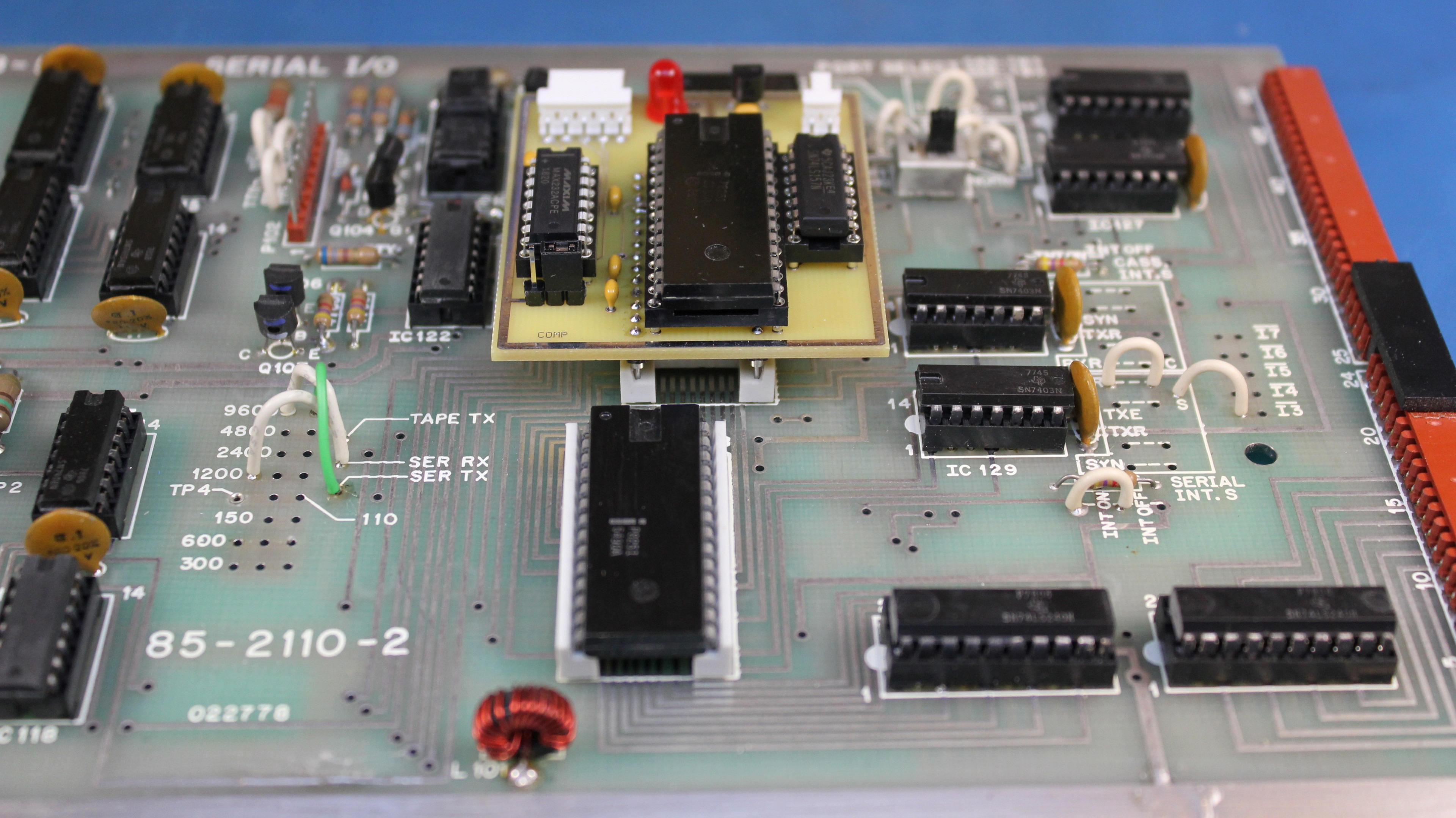
It tuned out the unused large mounting hole normally used by the analog 5 volt regulator could now be re-used as a board mounting hole to mount  the daughter board to an unused hold already on the H8-5 card. I only needed to place a threaded 4-40 x 1/2 inch nylon hex spacer between each of these two holes.

Wiring to the daughter board uses four 24AWG wires that are routed to solder points on the H8-5 card. These wire routes connect the +5V(red wire), ground(black wire), TxD signal(Gray wire) and RxD signal(orange wire). The solder locations used made sure that no foil on the H8-5 board needed to be cut.


The H8 Interface Board
To complete this modification several IC pins had to be disconnected and one IC had to be removed. These modifications are needed to prevent interference between the daughter board and the original tape interface electronics.

To disconnect an IC's pin, simply remove the IC from it's socket, carefully bend the needed pin very slightly out and finally re-install the IC back in to the socket making sure the pin to be disconnect does not go back in to the sockets hole. When done correctly the disconnected pin should just be on the outside of the IC socket.

The following list shows the removed IC and the disconnect pins needed:

Remove IC107
Disconnect IC112 pin 1
Disconnect IC108 pin 6
Disconnect IC117 pin 8

The final operation needed to complete this modification is placing a shorting jumper between pins 9 and 25 on IC123. This jumper is placed on the back side of the H8-5 board and hence is not visible in any of the pictures.

This jumper is needed to connect the received data clock (pin 25) to the baud rate clock already being used by the transmit data clock (pin 9).

The down side of this modification is the disabling of the tape interface itself. If we wished to use a tape recorder to save or load programs, we would have to reinstall the disconnected pins, reinstall the removed IC, remove the jumper on the back of the board and unplug the daughter board cable used to connect it to the H8-5.
The daughter board - a better solution for transferring H8T files between H8-5 Board and a PC
The H8-5-1 Daugher board
Click here to get the full PDF manual for the H8-5-1 Daughter Board project

My first attempt to in creating an RS232 serial interface used to transfer files between my H8 and a standard PC, used an existing board from one of my other projects. While this board did successfully create an interface, it required the removal of several integrated circuits on the H8-5 board. It also required the soldering of extra wires. This rendered the native cassette tape interface non-operational.
 
For me, this was unsatisfactory. Some form of interface system was need that allowed the H8-5 to be fully functional in both modes of operation. Tape interface and RS232 serial.
 
After reviewing the H8-5's schematic, the idea of creating a plugable daughter board seemed logical. This daughter board would replace the P8251 UASRT at location IC123.  

The resulting design is shown in the picture above.

Operation of the H8-5-1 Daughter Board is very simple. A sign SPST switch is used to select between normal Cassette Tape operation or using an external RS232 serial connection to a PC other serial data device. When the two pins on J102 are shorted the Tape mode is selected. Leaving the input on J102 open places the system in to serial transfer mode.

The red LED indicates the board is receiving +5 volt DC power.

The three pin jumper at JP101 may be used to generate a high or low RS232 signal output level at pin 4 of J101. This signal can then be used to place any handshake lines on an external serial data storage device into a required state

Refering to the sechamitc below for a circuit description.

IC102, C102 through C106, JP101 and J101  make up the RS232 serial interface circuit. The core of the interface is the MAX232A (IC102) integrated circuit.  RS232 level signals are routed through the 5-pin connector J101 to the MAX232A. Here the RS232 signal levels are converted to standard TLL or CMOS digital levels.  The four 0.1uF capacitors C103 through C106 are used by the MAX232A to create both a 5 volt to 10 volt voltage pump as well as a –10 volt inverter. While the pump/inverted combination can only source/sink a few milliamps, this is more than enough to handle most standard RS232 interfaces found on terminals or PCs.

Selectable jumper JP101 may be used to set up a RS232 high or low logic level on pin 4 of J101. This optional signal may be used to define a needed handshake inputs that might be needed while interfacing external serial device.

The final 0.1uF capacitor C102 is a simple power rail decoupling capacitor for IC102.  
IC103 and C103 make up the serial signal switching circuit. Serial signal switching is handled by a 74LS157 (IC103) quad 2 to 1 data selector integrated circuit. Serial data to and from the P8251 (IC101) along with the serial input clock are switched between ether the normal cassette interface electronics or the RS232 serial interface section handled by the MAX232 (IC102) described above.

Integrated circuit DS1233 (IC104), 10K ohm resistor R102 and a 0.001uF capacitors (C109) are used to create a switch debounce used by the incoming switching single received via 2-pin connector J102. This 3-pin, TO-92 cased integrated circuit is also used as a power on reset controller for the board. When power is applied, the DS1233 monitors the VCC supply until it reaches about 10% of 5 volts.  When VCC returns to an in-tolerance condition, the reset signal continues the active low state for approximately 350ms to allow the power supply to stabilize.

The 10K resistor R102 is used to pull high the switch input while 0.001uF capacitor C109 is used to help stabilize the switch debounce function on the DS1233. While the input to J102 is in the open state, the resulting control signal into the 74LS157 (IC103) pin 1 will be high selecting the external RS232 signaling. Shorting pins 1 and 2 on J102 will pull the DS1233 low placing 74LS157 (IC103) pin 1 low and selecting the normal internal cassette tape interface. Removing the short on J102 again allow the DS1233 to return the select signal to high after a pre-programmed debounce of 350mS.

The final 0.1uF capacitor C108 is a simple power rail decoupling capacitor for IC104.

The remaining IC101 socket is the P8251 integrated circuit removed from the original H8-5 circuit board and place on to the daughter board. For the circuit description of this component, refer to the Heathkit documentation supplied with the H8-5 board.

The H8-5-1 Daughter Board